Tilde 4.0 CHIP-Monks: Hardware implementation of CHIP-8
Written By Team CHIP-MonksCHIP-Monks
CHIP-Monks is a CHIP-8 system, an interpreted programming language, using Verilog, using it to simulate games such as Pong, Tetris, etc.
Mentees:
Mentors:
Introduction + Why CHIP-8
Long long ago, before the age of gaming as it is now, a revolutionary piece of technology emerged that empowered a generation of game developers - CHIP-8. It enabled gamers to make their software more portable.
CHIP-8 is an instruction set, running on a virtual machine. Its best feature is that it occupies very little memory allowing it to run on 8-bit microcomputers.
Inspired by this idea, our team worked on a project to create a CHIP-8 emulator using verilog.
Our project uses Verilog, a hardware description language (HDL), to implement the CHIP-8 instruction set. 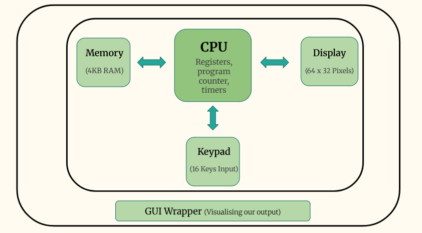
CHIP-8 Architecture
Coding in Verilog is like building blocks. Each block is referred to as a module and all these modules are coordinated using a top module as described in the figure:
Specs of Chip-8
-> Memory: CHIP-8 has direct access to up to 4 kilobytes of RAM
-> Display: 64 x 32 pixels (or 128 x 64 for SUPER-CHIP) monochrome, ie. black or white
-> A program counter, often called just “PC”, which points at the current instruction in memory One 16-bit index register called “I” which is used to point at locations in memory
-> A stack for 16-bit addresses, which is used to call subroutines/functions and return from them
-> An 8-bit delay timer which is decremented at a rate of 60 Hz (60 times per second) until it reaches 0
-> An 8-bit sound timer which functions like the delay timer, but which also gives off a beeping sound as long as it’s not 0
-> 16 8-bit (one byte) general-purpose variable registers numbered 0 through F hexadecimal, ie. 0 through 15 in decimal, called V0 through VF
-> VF is also used as a flag register; many instructions will set it to either 1 or 0 based on some rule, for example using it as a carry flag
CPU
→ CPU is the main part of Chip-8 which will be doing all of the calculations from loading up the sprites to saving data in the registers.
-> CPU will work under a clock signal which will help synchronise all of the elements in each of the modules modeled on Finite State Machine. FSM is a mathematical model of computation where the Finite State Machine is a small circuit that has a current state and changes to a next state depending on the inputs given to it.
This cycle consists of three core states:
- Fetch: The CPU retrieves two-byte instruction, called an OPCODE from memory.
- Decode: using a case statement to generate appropriate control signals for the execution stage.
- Execute: state will put instruction into action using registers, memory read and write or loading up sprites on display.
CPU has following components which will help it function:
-> Stack
- It stores the address the interpreter should return to after finishing with its instruction.
- It is an array of sixteen 16-bit value.
- Thus, it can handle the addresses for the next sixteen subroutines.
-> Timers
- Two timers are used in a CHIP-8 system, namely the sound timer and the delay timer.
- Both timers operate at 60hz and keep decrementing until 0, where the timers can be deactivated.
- Delay timer: Managing time events in the CHIP-8 system by controlling various delays among different events or actions.
- Sound timer: Managing sound events used by any program in CHIP-8, by emitting a single-tone beeping sound
-> Registers
- It is a in build memory for cpu that means it is located inside cpu, 16 8-bit general purpose registers are used, and these registers are numbered from 0 to F (0 to 16 in decimal) called V0 to VF.
- Registers are used to hold data that CPU is actively working on like sprites, values, addresses for stack.
OPCODE
-> OPCODE is a fancy term for Operation Codes (and that are instructions). We are using 33 Opcodes for Chip-8, all instructions are 2 bytes long and are stored most-significant-byte first. Opcode consists of four letters, usually MSB letter being a hex number which can be used to identify the Instruction.
-> Example of an OPCODE - 1NNN where 1 is a hex number and NNN can be a number or a letter. 1NNN is used to jump address, interpreter sets the Program counter to address NNN. Where first byte 1N is stored at address 0x200 and the other byte at NN and then combined to form a instruction inside the cpu, executing stage will use first letter of the opcode to find the execution sequence.
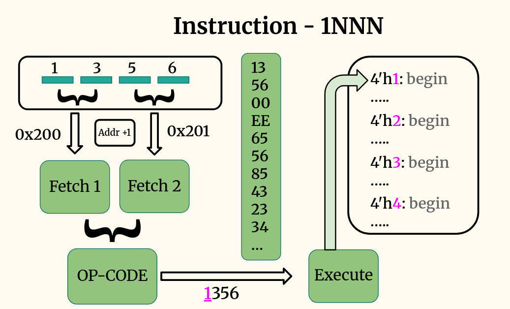
Instruction 1NNN
-> In memory, the first byte of each instruction (2 letters) should be located at an even address. If a program includes sprite data, it should be padded so any instructions following it will be properly situated in RAM
-> Here are the OPCODES we implemented
Memory
-> CHIP-8 systems have a total memory of 4096 bytes (or 4KB), from 0x000 to 0xFFF
-> It is divided into primarily two sections: - Reserved Memory (512 bytes) - Program Memory (4.5KB)
-> Reserved Memory (0x000 to 0x1FF), is used for the CHIP-8 interpreter as well as the fontset in the system.
-> Usually, the first 80 bytes is reserved for the font-set, which is where we store our characters. These are the characters used on the display, from letters A-F and numbers 0-9.
-> From 0x200 to 0xFFF, the rest of the memory is for Program memory.
Display
-> The display of CHIP-8 can be thought of as a matrix of pixels. It has 64x32 pixels that form a monochrome grid. This means that there are no colors to manage, each pixel exists in only two states: ON or OFF.
-> The working of the display is implemented by the use of the XOR gate. Looking at the truth table of the XOR gate, the truth table explains every possible value a pixel can take :
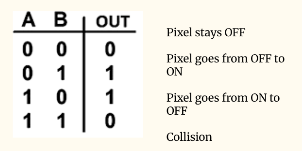
Display Pixel Logic
-> The state of collision is when a pixel which is ON is once again given an ON signal. In this case, the pixel is erased, i.e, it turns OFF
-> This is an incredible concept as it not only draws pixels onto the screen, but it also provides a collision detection mechanism. This feature is fundamental for programming classic games like Pong or Space Invaders, where detecting if two objects have collided is a major part of the gaming logic.
-> All graphics in CHIP-8 are rendered using sprites. A sprite can be defined as a small graphical image or pattern that could be up to a maximum of 15 bytes.
-> In order to understand what this boundary condition implies, we must first understand that in CHIP-8, a sprite is always 8 pixels wide, corresponding perfectly to a single byte. This width is fixed. What varies is the number of rows, this corresponds to the height of the sprite which is limited to 15 bytes.
-> To better understand this, let us look at an example of a sprite for the letter ‘A’:
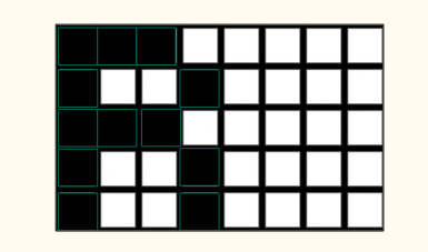
Letter A
[0x3C,
0x42,
0x7E,
0x42,
0x42]
-> Each hexadecimal code is converted to its corresponding binary equivalent which correlates to which pixels are turned ON and which remain OFF.
-> To bring these sprites to life on the screen, CHIP-8 uses the following opcode : DXYN.
This stands for :
D - Draw command.
X - Horizontal coordinate
Y - Vertical coordinate
N - Number of bytes (rows)
By executing this single command, the emulator can render complex characters and graphics, which is the visual foundation of any game.
Display Pipeline
→ After connecting CPU, Memory and Display to TOP module, we verified display module. To do that we initialized Memory with sprite data from a .mem file. We checked the functionality and CPU successfully fetched the sprite data and passed to display module.
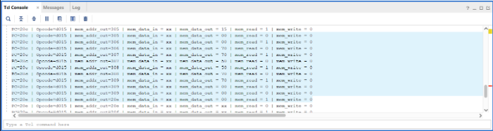
Data flowing from CPU to Display module
Here we are verifying that data is flowing from the cpu to display module
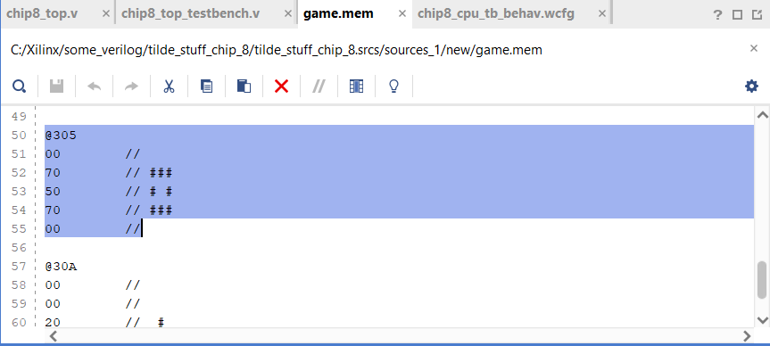
Sprite data stored in game.mem
Here this image shows the .mem file which is used to store the testing instructions and sprites.
What’s Next ?
To further build on this project, we would be exploring the following:
- Desktop Simulation with Verilator and RayLib:
Verilator is an open-source Verilog simulator used to compile hardware designs to run natively on the system. This along with the RayLib graphics library which is used to create graphics is a good way to improve the graphics and rendering of the project.
- Create a Parameterized Game Engine:
By parameterizing elements such as the display width, game speed, or obstacle density, the code becomes more reusable and adaptable to different set ups.
- FPGA Synthesis:
The final step to truly realise the capabilities of a HDL - implementation on an FPGA. This requires the code to be fully synthesizable. This step can bring our project from the simulation level to a hardware implementation!